
PCB Assemblies
Printed circuit boards (PCBs) are much more than just thin, hard surfaces with printed electronic circuits. They serve as the lifeline of your electronic device’s operating system. At RSP, we understand the intricate complexities and critical role that PCBs play in the functionality and performance of electronic devices. RSP electrical engineers optimize the PCB layout and design, carefully select the materials and components, and employ advanced manufacturing techniques to achieve exceptional results.

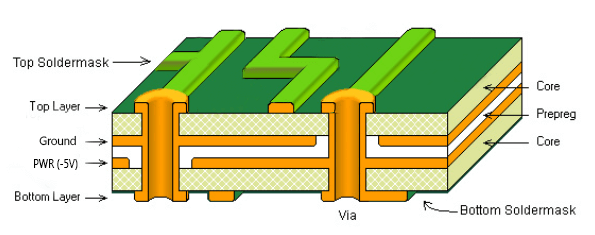
PCB Layers and Design
Printed circuit boards (PCBs) can have varying numbers of layers depending on the complexity and functionality of the electronic device they are designed for. PCBs can range from single-layer boards to multilayer boards with numerous layers stacked together. The standard layers range from one to eight, but many more are possible.
Single-layer PCBs are commonly used in simple electronic devices with fewer components and less complex circuitry. Double-layer PCBs provide increased flexibility in circuit design and are suitable for more complex electronic devices. Additional layers are used for the most complex designs.
The functionality of different layers in a multilayer PCB depends on their specific purpose in the circuit design and on how complex that design must be. Here are some common types of layers found in multilayer PCBs:
- Signal layers: These layers contain the conductive traces that carry electrical signals between different components and circuitry on the PCB. Signal layers are responsible for the main functionality of the PCB, transmitting data, power and control signals.
- Power planes: These layers are dedicated to providing power supply to various components on the PCB. Power planes ensure stable and efficient distribution of power throughout the circuit, reducing noise and interference.
- Ground planes: Ground planes act as a reference point for electrical signals and provide a stable ground connection for components. They help minimize electromagnetic interference (EMI) and improve signal integrity.
- Internal layers: Multilayer PCBs may have additional internal layers that are not accessible from the outside. These layers may contain traces or planes for specific purposes, such as impedance control, high-speed signal routing or thermal management.
Printed Circuit Board Assembly and Manufacturing
For expertise in printed circuit boards (PCBs), copper flex circuits (FCPs), flexible boards and printed circuit board assemblies (PCBAs), look no further than RSP, a leading manufacturer of printed circuit boards.
At RSP, we understand the importance of versatility in product design and operation, and our flexible boards are designed precisely for that purpose. With our extensive experience in PCB manufacturing, we provide the expertise you need to bring your product from the idea stage to full realization. We guide you through every step of the process, ensuring seamless execution and outstanding results.

Our full-service electronic solutions encompass highly experienced engineering teams in both the US and China. We leverage their skills and knowledge to ensure that your products are brought to life with utmost precision and efficiency.
With our strategic location in China, we offer low- and high-volume production services for PCB assembly. Our commitment to matching customer needs with optimal resources and staffing ensures that your PCB assembly is handled with the care and expertise we’re known for.
Our innovative engineering teams offer a diverse range of capabilities to meet your specific requirements. Whether you need single-layer, double-layer or multilayer circuit boards, RSP has the expertise to deliver the precise solutions you need. Additionally, we collaborate with several domestic engineering companies, further expanding the depth and breadth of our services.
Before the PCB Process
Before manufacturing a printed circuit board assembly (PCBA), several crucial steps are typically undertaken to ensure smooth and successful production. Here’s a brief overview of the key steps:
- Design and Engineering: The initial step involves designing the PCBA, including the schematic and layout of the circuit board.
- Design for Manufacturability (DFM) Analysis: A DFM analysis is performed to assess the manufacturability of the PCBA design.
Prototyping and Validation: A prototype of the PCBA is typically manufactured to verify the design’s functionality and performance. This step allows for testing, debugging and making any necessary adjustments or improvements before moving to full-scale production.- Quality Control and Testing: Quality control measures are implemented throughout the manufacturing process to ensure the PCBA’s adherence to specifications and standards. Testing procedures are defined and executed and may include functional testing, in-circuit testing (ICT) or automated optical inspection (AOI), among others.
PCB Process
The process of making a PCBA involves several essential steps that transform the PCB design into a functional electronic device. The manufacturing process may vary slightly depending on the complexity of the PCBA design and specific customer requirements. Here’s a brief overview of the typical PCBA manufacturing process:
- Component Preparation: The required components are prepped for the PCBA.
- PCB Fabrication: The printed circuit board is fabricated by etching a copper-clad substrate, typically made of fiberglass or composite material. The board is cut to the desired size and shape, and copper layers are added to create the required circuitry.
- Solder Paste Application: Solder paste, a mixture of tiny solder particles and flux, is applied to the surface of the PCB. This paste is used to create solder joints between the components and the PCB during the assembly process.
- Component Placement: Automated assembly machines or manual labor is employed to accurately place the electronic components onto the PCB.
- Soldering: The entire board is heated to a controlled temperature, causing the solder paste to melt and form secure electrical connections between the components and the PCB.
- Inspection and Testing: Various inspection techniques are employed to ensure the quality and functionality of the PCBA. Automated optical inspection (AOI), X-ray inspection and functional testing are conducted to identify any defects or faults.
- Cleaning: The PCBA is cleaned to remove any flux residue or contaminants that might affect its performance.
- Post-Assembly Rework: If any defects are identified during inspection or testing, necessary rework is performed to rectify the issues.
- Final Testing: The completed PCBA undergoes comprehensive testing to verify its functionality, its performance and its compliance with the required specifications. This testing may involve functional testing, in-circuit testing (ICT)or other specific tests based on the device’s intended purpose.
- Packaging and Delivery: The PCBA is carefully packaged to protect it during transportation.
Our PCBA capabilities are vast and diverse. In addition to electronic manufacturing services, RSP also offers high-density, complex SMT (surface mount technology where components are placed outside the circuit board); in-circuit testing (ICT); functional testing (FT); burn-in; RoHS lead-free testing; and SPC and Process Control Systems.
RSP is certified in ISO 9001 and works with outside partners certified in ISO 14001, TS 16949, QS9000 and BABT.
Additional Services
Our expertise extends beyond PCB manufacturing. We provide full-contract manufacturing services to seamlessly move your product from concept to production, as well as mechanical engineering services, leveraging our skilled team to assist you in all aspects of product development. From initial design concepts to prototyping, testing and turnkey assembly, we work closely with you to bring your ideas to life.
RSP understands the importance of flexibility and innovation. Our experience in producing low-volume quantities and prototypes enables us to cater to a wide range of customer needs. We empower you to explore new product ideas and bring them to market, allowing for unparalleled innovation and creativity.
In addition to our core offerings, RSP also specializes in box builds and integrated systems design. We tailor our services to meet your product’s unique requirements and stage of development, providing you with a comprehensive solution under one roof.